A squeezing mission in the field of nanoelectronics is the quest for a material that could supplant silicon. Graphene has appeared to be encouraging for quite a long time. In any case, its true capacity has vacillated en route because of harmful handling strategies and the absence of another gadget worldview to embrace it. With silicon almost at its maximum in its capacity to oblige quicker registration, the next enormous nanoelectronics stage is required now like never before.
Walter de Heer, officials’ teacher in the School of Material Science at the Georgia Foundation for Innovation, has moved forward in presenting the case for a replacement for silicon. De Heer and his partners have fostered a new nanoelectronics stage in light of graphene, a solitary sheet of carbon particles. With traditional microelectronics manufacturing, there is a need for any viable alternative to silicon.
Throughout their examination, distributed in Nature Correspondences, the group might have likewise found another quasiparticle. Their disclosure could lead to the development of more modest, faster, more effective, and less expensive microchips, as well as implications for quantum and elite execution figuring.
“Quantum interference has been detected in carbon nanotubes at low temperatures, and we expect to see comparable effects with epigraphene ribbons and networks. This key property of graphene is not possible with silicon.”
Walter de Heer, Regents’ Professor in the School of Physics
“Graphene’s power lies in its level, two-layered structure that is kept intact by the most grounded compound bonds known,” de Heer said. “It was obvious from the very outset that graphene can be scaled down to a far more noteworthy degree than silicon, empowering a lot more modest gadgets while working at higher paces and creating substantially less intensity.” This essentially implies that more gadgets can be crammed onto a single graphene chip than silicon.
In 2001, de Heer proposed an elective type of hardware in light of epitaxial graphene, or epigraphene—aa layer of graphene that was found to immediately frame on top of silicon carbide, a semiconductor utilized in high-power gadgets. At that point, specialists found that electric flows stream without opposition along graphene’s edges and that graphene gadgets could be consistently interconnected without metal wires. This mix takes into consideration a type of gadget that depends on the unique light-like properties of graphene electrons.
“Quantum impedance has been seen in carbon nanotubes at low temperatures, and we hope to see comparative impacts in epigraphene strips and organizations,” de Heer said. “This significant component of graphene is preposterous with silicon.”
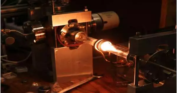
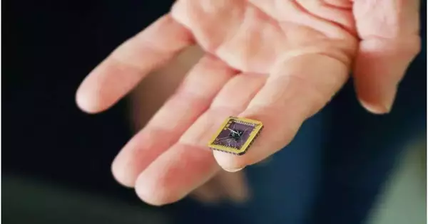
Licensed acceptance heaters at Georgia Tech were used to create graphene on silicon carbide.
Building the stage
To make the new nanoelectronics stage, the specialists made a different type of epigraphene on a silicon carbide gem substrate. They created one-of-a-kind silicon carbide chips from device-grade silicon carbide gems in collaboration with scientists at the Tianjin International Place for Nanoparticles and Nanosystems at the University of Tianjin in China.The graphene itself was developed at de Heer’s research center at Georgia Tech, utilizing licensed heaters.
The specialists utilized electron shaft lithography, a strategy usually utilized in microelectronics, to cut the graphene nanostructures and weld their edges to the silicon carbide chips. This interaction precisely balances out and seals the graphene’s edges, which would somehow respond with oxygen and different gases that could slow down the movement of the charges along the edge.
At long last, to quantify the electronic properties of their graphene stage, the group utilized a cryogenic device that permitted them to record its properties from a temperature as close to zero as possible to room temperature.
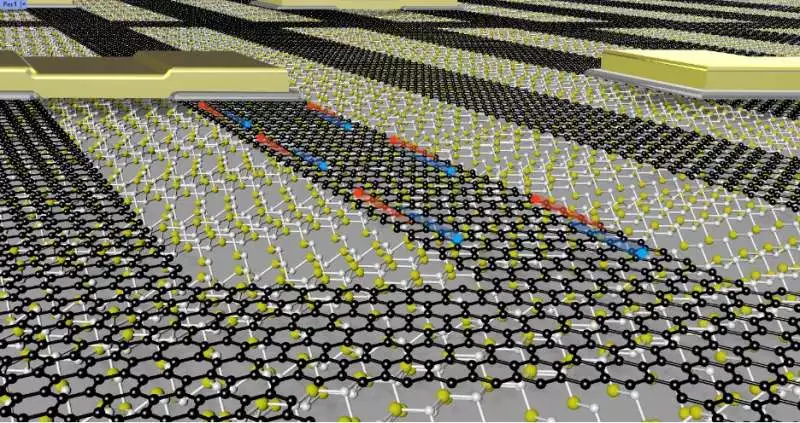
The graphene network (dark particles) is depicted on top of silicon carbide (yellow and white molecules).The gold cushions address electrostatic doors, and the blue and red balls address electrons and openings, individually.
Observing the edge state
The electric charges the group saw in the graphene edge state were like photons in an optical fiber that can go over huge distances without dissipating. They found that the charges went for a huge number of nanometers along the edge prior to dissipating. Graphene electrons in past advances could go around 10 nanometers before catching little blemishes and dispersing every which way.
“What’s exceptional about the electric charges in the edges is that they stay on the edge and continue to go at a similar speed, regardless of whether the edges are entirely straight,” said Claire Berger, material science teacher at Georgia Tech and head of examination at the French Public Community for Logical Exploration in Grenoble, France.
In metals, electric flows are conveyed by adversely charged electrons. In any case, in opposition to the specialists’ assumptions, their estimations recommended that the edge flows were not conveyed by electrons or by openings (a term for positive quasiparticles demonstrating the shortfall of an electron). Rather, the flows were conveyed by an exceptionally surprising quasiparticle that has no charge and no energy but moves without opposition. The parts of the cross-breed quasiparticle were seen to go on the inverse sides of the graphene’s edges, in spite of being a solitary item.
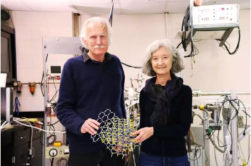
Walter de Heer and Claire Berger hold a nuclear model of graphene (dark iotas) on translucent silicon carbide (yellow molecules) in the epitaxial graphene lab at Georgia Tech.
The special properties demonstrate that the quasiparticle may be one that physicists have been wanting to take advantage of for quite a long time—the tricky Majorana fermion anticipated by Italian hypothetical physicist Ettore Majorana in 1937.
“Creating gadgets involving this new quasiparticle in flawlessly interconnected graphene networks is downright revolutionary,” de Heer said.
It will probably be another five to 10 years before we have the first graphene-based gadgets, as per de Heer. Be that as it may, on account of the group’s new epitaxial graphene stage, innovation is closer than at any time in recent memory to delegating graphene as a replacement to silicon.
More information: Vladimir S. Prudkovskiy et al, An epitaxial graphene platform for zero-energy edge state nanoelectronics, Nature Communications (2022). DOI: 10.1038/s41467-022-34369-4
Journal information: Nature Communications


