On sports television channels, a slow-motion movie depicts processes in hundredths of a second. By contrast, processes on the nanoscale take place in the so-called femtosecond range: For example, an electron needs only billionths of a second to orbit a hydrogen atom.
Physicists around the world are using special instruments to capture such ultrafast nanoprocesses in films. Researchers at Kiel University (CAU) have developed a new method for such films that is based on a different physical concept and thus allows for further and more precise options for investigation.
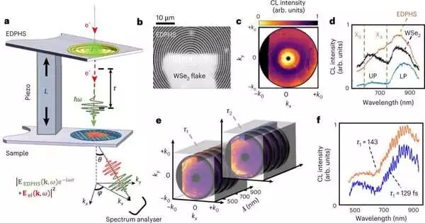
To do this, they combined an electron microscope with nanostructured metallic thin films that generate very short light pulses. They were thus able to film the coherent interactions of light and electrons in a semiconductor in a first experiment.Their results are published in Nature Physics.
The new method is simpler and more cost-effective.
Until now, movies showing ultrafast nanoprocesses have typically been produced using high-power lasers combined with electron microscopes. But only a few research groups can afford such large and complex setups. “Our concept does not require expensive and complicated lasers and can be easily replicated,” says Nahid Talebi, Professor of Experimental Physics at the CAU.
Electron microscopes bundle electrons into a beam, accelerate it, and direct it at a material sample. Conclusions about the properties of the materials and the processes inside can be drawn based on how electrons pass through or are reflected in the sample.
“Electron microscopes have a significantly better spatial resolution than optical microscopes and make investigations in the nanometer range possible in the first place,” says Talebi. The special components she has developed make it relatively easy to improve the temporal resolution of electron microscopes and convert them to their ultrafast versions. By this means, nanoscale processes can now also be captured in ultrafast films on the femtosecond time scale without lasers.
With her new publication, Talebi not only demonstrates that her method works. Together with her research associate, Dr. Masoud Taleb, she also provides experimental evidence for coherent interactions of photons and electrons in a semiconductor, which had previously only been described theoretically. The quantum material tungsten diselenide, WSe2, used for this purpose originates from a collaboration with Professor Kai Rossnagel within the priority research area KiNSIS (Kiel Nano, Surface, and Interface Science) at Kiel University.
Nano-structured metal generates short light pulses.
A central component of Talebi’s concept is a special nanostructure that looks similar to a kitchen sieve. It can be inserted into an electron microscope, where it functions like a light source, called an “EDPHS” (electron-driven photon source). When an electron beam hits this metal structure, the hole pattern generates targeted, short light pulses that can be used to make fast films.
The researchers drilled tiny holes ranging from 25 to 200 nanometers into a thin gold foil to create the unique structure. Because light pulses only occur with a specific hole pattern, Talebi had precisely calculated the sizes and distances. The “nanosieves” were produced in close collaboration with Dr. Mario Hentschel from the research group of Prof. Harald Giessen, University of Stuttgart.
Together with colleagues from Amsterdam, Talebi had previously modified the electron microscope so that it could detect cathodoluminescence. These light signals are generated when fast electrons hit metal.
Interactions between electrons and photons are documented in films.
In the experiment described in the current publication, the short light pulses from the sieve-like nanostructures hit the semiconductor sample at the speed of light. Here they excite excitons, so-called quasiparticles.
These are electrons that have detached themselves from an atom and are still coupled to the hole they created (“electron-hole pairs”). “If, a short time later, the slower electron beam also hits the semiconductor sample, we can see from the reaction of the electrons how the excitons have behaved in the meantime,” explains Talebi.
The resulting cathodoluminescence signals from the superposition of the electron beam and the light pulses show a coherent interaction between electrons and photons.
To be able to capture these processes on film, the researchers also integrated a piezoelectric crystal into the microscope setup. This allows them to precisely change the spatial distance between the light source and the sample and, by extension, the temporal distance between the incident light pulses and the electrons. “In this way, images can be taken at different stages of the process and assembled into a film,” Talebi summarizes.
More information: Nahid Talebi, Phase-locked photon–electron interaction without a laser, Nature Physics (2023). DOI: 10.1038/s41567-023-01954-3. www.nature.com/articles/s41567-023-01954-3


