The quantum twisting microscope (QTM) is a cutting-edge tool for studying the electronic and magnetic properties of materials at the atomic scale. It was first proposed in 2018 by researchers at Harvard University and MIT, and has since been developed and used by several research groups around the world.
One of the most intriguing aspects of the quantum world is that a particle, such as an electron, is also a wave, which means it can exist in multiple places at the same time. Researchers from the Weizmann Institute of Science use this property in a new study published today in Nature to develop a new type of tool, the quantum twisting microscope (QTM), that can create novel quantum materials while simultaneously peering into the most fundamental quantum nature of their electrons. The study’s findings could be used to develop electronic materials with previously unseen capabilities.
The QTM involves “twisting” or rotating two atomically thin layers of material in relation to one another. Such twisting has become a major source of discoveries in recent years. It all started with the discovery that stacking two layers of graphene, one-atom-thick crystalline sheets of carbon, one on top of the other with a slight relative twist angle results in a “sandwich” with surprising new properties.
The twist angle proved to be the most important parameter for controlling electron behavior: changing it by one-tenth of a degree could transform the material from an exotic superconductor to an unusual insulator. However, as critical as it is, this parameter is also the most difficult to control in experiments. Generally, twisting two layers to a new angle necessitates creating a new “sandwich” from scratch, which is a time-consuming and labor-intensive process.
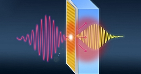
The trick for seeing quantum waves is to spot the same electron in different locations at the same time. The measurement is conceptually similar to the famous two-slit experiment, which was used a century ago to prove for the first time that electrons in quantum mechanics have a wave nature.
Alon Inbar
“Our original motivation was to solve this problem by building a machine that could continuously twist any two materials with respect to one another, readily producing an infinite range of novel materials,” says team leader Prof. Shahal Ilani of Weizmann’s Condensed Matter Physics Department. “However, while building this machine, we discovered that it can also be turned into a very powerful microscope, capable of seeing quantum electronic waves in ways that were unimaginable before.”
Creating a quantum picture
Images have long played an important role in scientific research. Light microscopes and telescopes routinely provide images that help scientists understand biological and astrophysical systems better. Taking pictures of electrons inside materials, on the other hand, has been notoriously difficult for many years due to the small dimensions involved. This changed 40 years ago with the invention of the scanning tunneling microscope, which earned its creators the Nobel Prize in Physics in 1986. This microscope scans the surface of a material with an atomically sharp needle, measuring the electric current and gradually building an image of the distribution of electrons in the sample.
“Since this invention, many different scanning probes have been developed, each measuring a different electronic property, but all of them measure these properties at the same location at the same time. As a result, they mostly see electrons as particles and can only infer their wave nature indirectly “Prof. Ady Stern of the Weizmann Institute, who participated in the study with three other theoretical physicists from the same department, Profs. Binghai Yan, Yuval Oreg, and Erez Berg, explains. “As it turns out, the tool we built can directly visualize the quantum electronic waves, giving us a way to unravel the quantum dances they perform inside the material,” Stern says.
Spotting an electron in several places at once
“The trick for seeing quantum waves is to spot the same electron in different locations at the same time,” says Alon Inbar, a lead author on the paper. “The measurement is conceptually similar to the famous two-slit experiment, which was used a century ago to prove for the first time that electrons in quantum mechanics have a wave nature,” adds Dr. John Birkbeck, another lead author. “The only difference is that we perform such an experiment at the tip of our scanning microscope.”
To accomplish this, the researchers replaced the scanning tunneling microscope’s atomically sharp tip with a tip containing a flat layer of a quantum material, such as a single layer of graphene. When this layer comes into contact with the surface of the sample of interest, it creates a two-dimensional interface through which electrons can tunnel in a variety of ways. They tunnel in all locations at the same time, and the tunneling events at different locations interfere with each other. Only when the wave functions on both sides of the interface match exactly can an electron tunnel.
“To see a quantum electron, we have to be gentle,” says Ilani. “If we don’t ask it the rude question ‘Where are you?’ but instead provide it with multiple routes to cross into our detector without us knowing where it actually crossed, we allow it to preserve its fragile wave-like nature.”
Twist and tunnel
The electronic waves in the tip and the sample generally propagate in opposite directions and thus do not match. The QTM’s twisting ability is used to determine the angle at which matching occurs: The tool causes their corresponding wave functions to twist with respect to one another by continuously twisting the tip with respect to the sample. Tunneling can occur when these wave functions match on both sides of the interface.
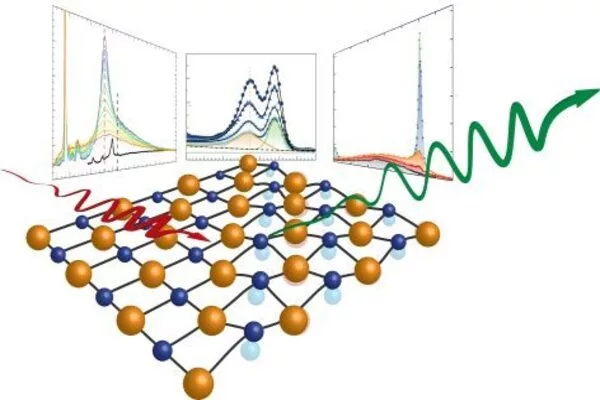
Similarly to how lateral translations of the tip enable mapping of its dependence on position, twisting allows the QTM to map how the electronic wave function depends on momentum. Simply knowing the angles at which electrons cross the interface provides the researchers with a wealth of information about the probed material. In this manner they can learn about the collective organization of electrons within the sample, their speed, energy distribution, patterns of interference and even the interactions of different waves with one another.
A new twist on quantum materials
“Our microscope will give scientists a new kind of ‘lens’ for observing and measuring the properties of quantum materials,” says Jiewen Xiao, another lead author.
The Weizmann team has already used their microscope to study the properties of several key quantum materials at room temperature, and they are now planning new experiments at temperatures as low as a few kelvins, where some of the most exciting quantum mechanical effects are known to occur.
Peering so deeply into the quantum world can aid in the discovery of fundamental natural truths. It may also have a significant impact on emerging technologies in the future. The QTM will give researchers unprecedented access to a wide range of new quantum interfaces, as well as new “eyes” for discovering quantum phenomena within them.