Throughout the course of recent years, material researchers and hardware engineers have been attempting to manufacture new adaptable inorganic materials to make stretchable and exceptionally performing electronic gadgets. These gadgets can be founded on various plans, like inflexible island dynamic cells with serpentine-shape or fractal interconnections, nonpartisan mechanical planes, or bunched structures.
In spite of the critical advances in the manufacture of stretchable materials, a few difficulties have proven challenging to overcome. For example, materials with wavy or serpentine interconnect patterns generally have a restricted region thickness, and it is frequently both troublesome and costly to create proposed stretchable materials. Also, the firmness of many existing stretchable materials doesn’t match that of human skin tissue, making them anxious on the skin and, in this way, not great for making wearable advances.
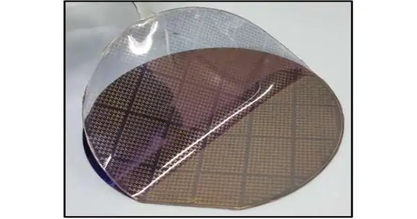
Scientists at Sungkyunkwan College (SKKU), the Foundation for Essential Science (IBS), Seoul Public College (SNU), and the Korea Progressed Establishment of Science and Innovation (KAIST) have as of late created a vacuum-stored versatile polymer for creating stretchable hardware. This material, presented in Nature Gadgets, could be utilized to make stretchy field-impact semiconductors (FETs), which are essential parts of most electronic gadgets available today.
“In our research, we provide a novel approach to the design of dielectric materials to address the aforementioned problems in inherently stretchable electrical devices,”
Donghee Son, one of the researchers who carried out the study,
“As of late, different methodologies for taking on delicate materials have been proposed for growing naturally stretchable gadgets, which needn’t bother with a particular underlying model inferable from their inborn deformability,” Donghee Child, one of the specialists who did the review, told Tech Xplore. “However, such gadgets utilized arrangement-handled dielectric materials and thus encountered fundamental difficulties in achieving high electrical exhibitions.”
Arrangement-handled natural entryway dielectric materials, materials that can communicate power without directing it (i.e., protecting it), are not especially reasonable for the production of adaptable hardware. Most prominently, they have thicknesses in the micrometer range, poor protecting exhibitions, substance shakiness, and low consistency. Similarly, they are typically incompatible with conventional microfabrication processes, making them difficult to create on a large scale.
Because of these impediments, electronic parts in these arrangement-handled materials are tormented by unfortunate door controllability and high activity voltages, as well as a restricted versatility. Child and his colleagues, along with other research groups around the world, have been attempting to make ultrathin, stretchable, adaptable, and highly performing dielectrics using alternative manufacturing techniques.
“In our review, we present another approach to dealing with the problem of dielectric materials in order to determine the previously mentioned difficulties in characteristically stretchable electronic devices,” Child explained. “Our huge scope of vacuum-saved stretchable dielectrics empowers the versatile manufacture of characteristically stretchable gadgets with electrical exhibitions tantamount to those created utilizing the non-stretchable inorganic and stretchable natural dielectric materials (e.g., Al2O3 stored by means of a nuclear layer statement and a twist-covered viscoelastic layer).”
Picture of inherently stretchable semiconductors and rationale for doors utilizing a vacuum-saved polymer dielectric.
To make their polymer-based dielectric, Child and his partners initially copolymerized two unique monomers, specifically isononyl acrylate (INA) and 1,3,5-trimethyl-1,3,5-tryvinyl cyclotrisiloxane (V3D3), utilizing an interaction known as the synthetic fume effect (iCVD). The monomer INA acts as a delicate portion, expanding the material’s stretchability, while V3D3 fills in as a cross-linkable hard fragment, giving the polymer film vigorous protecting properties.
“The blending proportion of the monomers (INA and V3D3) was improved to accomplish both protecting and extending the execution of the gadget,” Child said. “Our vacuum-saved polymer dielectric with a dielectric steady of 3.59 and a breakdown field of 2.3 MV/cm showed the same oxide thickness (EOT) of under 200 nm, which is the most minimal worth among the stretchable dielectric layers tested to date.”
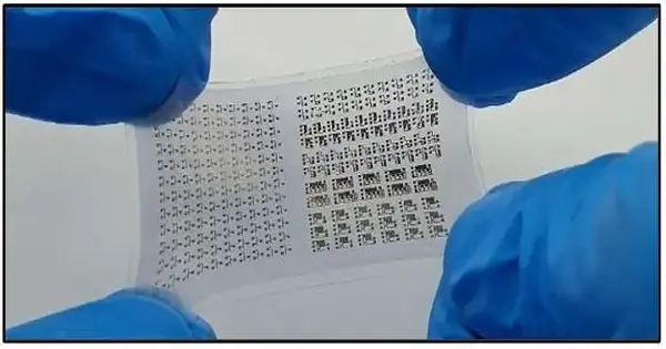
To demonstrate the durability of their material, the experts used it to create semiconductors, which were then used to create stretchy inverters and rationale doors.In starting tests, these parts accomplished exceptionally encouraging outcomes.
Notwithstanding a high dielectric constant and a low EOT value, they could be extended up to a 40% strain while holding their protecting presentation. The group likewise found that their material shows high substance and warmth during microfabrication cycles and remains profoundly uniform over huge regions.
“Our own is the principal record of a vacuum-stored stretchable dielectric, likewise showing its application to characteristically stretchable electronic gadgets,” Child said. “At the end of the day, looking at traditional thick polymer dielectrics, a stretchable, vacuum-saved, nanometer-thick film (roughly 160 nm) has outstanding electrical, mechanical, and substance properties. The remarkable advantages inherent in our vacuum-stored technique could aid in the advancement of high-performance wafer-adaptable wearable gadgets.”The perceptions of our review would change the regular worldview of delicate gadgets.”
Later on, the material developed by the group could enable the development of new, uniquely stretchable and profoundly performing semiconductors and rational circuits that consume less electrical power.These semiconductors and circuits could be utilized to make various delicate gadgets, including wearable and implantable gadgets.
“I believe the main issue in the long-term advancement of reliable wearables will be achieving an energy-efficient execution in stretchable electronic gadgets,” Child added. “In this way, the thickness of the vacuum-kept protecting materials ought to be progressively more slender, to further develop entryway controllability while keeping up with stretchability.” Moreover, its dielectric consistency would be superior up to about 10, which is equivalent to that of the great K inorganic dielectric.”
More information: Ja Hoon Koo et al, A vacuum-deposited polymer dielectric for wafer-scale stretchable electronics, Nature Electronics (2023). DOI: 10.1038/s41928-023-00918-y.
Journal information: Nature Electronics


