Specialists at the Korea Exploration Foundation of Norms and Science fostered a poisonous gas sensor with the world’s most noteworthy responsiveness. This sensor can definitively screen nitrogen dioxide (NO2), a poisonous gas in the air, at room temperature with low power utilization and super-high responsiveness. It tends to be applied to different fields, for example, the location of leftover gases during the semiconductor production cycle and the examination of electrolysis impetuses.
NO2, created by the high-temperature burning of petroleum derivatives and principally discharged through auto fumes or processing plant smoke, adds to an expansion in mortality because of air contamination. In South Korea, the yearly typical centralization of NO2 in the air is directed to be 30 ppb or lower by official declaration. Exceptionally delicate sensors, in this manner, are expected to identify gases at very low fixations precisely.
Lately, the utilization of poisonous gases that are possibly lethal to people has been on the ascent because of the advancement of cutting-edge ventures, including semiconductor fabrication. While certain labs and production lines have embraced semiconductor-type sensors for security, the test lies in their low reaction responsiveness, making them unfit to recognize poisonous gases that might try and be detectable to the human nose. To expand their responsiveness, they consume a great deal of energy in the end since they should work at high temperatures.
“This technology, which overcomes the limitations of traditional gas sensors, will not only meet government regulations, but will also allow for more precise monitoring of domestic atmospheric conditions. We will do additional research so that this technology can be used to produce various dangerous gas sensors and catalysts that go beyond monitoring NO2 in the atmosphere.”
Dr. Jihun Mun, a senior researcher of the KRISS Semiconductor Integrated Metrology Team,
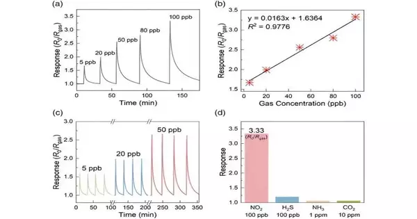
The recently evolved sensor, a cutting-edge semiconductor-type harmful gas sensor in view of cutting-edge materials, shows essentially further developed execution and ease of use compared with traditional sensors. With its remarkable aversion to compound responses, the new sensor can identify NO2 considerably more delicately than recently revealed semiconductor-type sensors, a responsiveness that is multiple times higher. Also, the original sensor consumes insignificant power working at room temperature, and its ideal semiconductor producing process empowers huge region union at low temperatures, in this way decreasing creation costs.
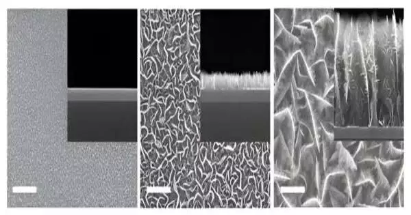
Flowing interaction for making 3D MoS2 nano-branches. The primary change of MoS2 into a 3D tree-limb shape can be seen over time. Credit: Korea Exploration Organization of Norms and Science (KRISS)
The way into innovation lies in the MoS2 nanobranch material created by KRISS. Dissimilar to the regular 2D-level construction of MoS2, this material is combined in a 3D design looking like tree limbs, consequently upgrading the responsiveness. Other than its solidarity of uniform material combinations on an enormous region, it can make a 3D design by changing the carbon proportion in the natural substance without extra cycles.
The KRISS Semiconductor Coordinated Metrology Group has tentatively shown the way that their gas sensor can identify NO2 in the environment at fixations as low as 5 ppb. The determined location breaking point of the sensor is 1.58 ppt, denoting the world’s most significant level of responsiveness.
This accomplishment empowers the exact observation of NO2 in the climate with low power utilization. The sensor saves time and money as well as offers a magnificent goal. It is normal to investigate climatic circumstances by identifying yearly normal centralizations of NO2 and observing constant changes.
One more quality of this innovation is its capacity to change the carbon content of the natural substance during the material union stage, accordingly modifying the electrochemical properties. This can be used to foster sensors equipped for recognizing gases other than NO2, for example, lingering gases delivered during semiconductor-producing processes. The brilliant synthetic reactivity of the material can likewise be taken advantage of to improve the exhibition of electrolysis impetuses for hydrogen creation.
Dr. Jihun Mun, a senior specialist of the KRISS Semiconductor Coordinated Metrology Group, said, “This innovation, which conquers the limits of customary gas sensors, won’t just meet unofficial laws yet additionally work with exact checking of homegrown air conditions. We will proceed with follow-up research with the goal that this innovation can be applied to the advancement of different poisonous gas sensors and impetuses, stretching beyond the observation of NO2 in the air.”
More information: Jeongin Song et al. MOCVD of Hierarchical C‐MoS2 Nanobranches for ppt‐Level NO2 Detection, Small Structures (2023). DOI: 10.1002/sstr.202200392


