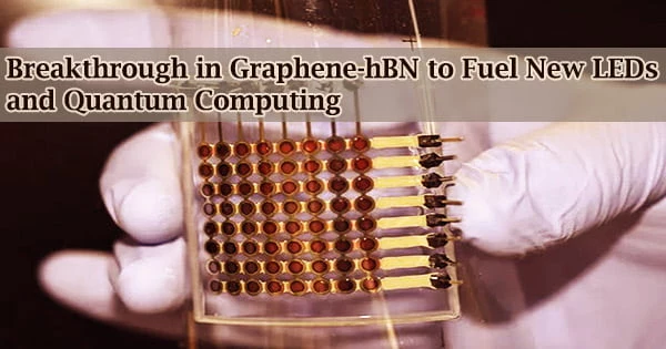
A University of Michigan research team has created the first reliable, scalable method for generating single layers of hexagonal boron nitride on graphene, which might speed up research into next-generation electronics and LED devices.
A research published in Advanced Materials details the approach, which can generate enormous sheets of high-quality hBN using the commonly utilized molecular-beam epitaxy method.
According to Zetian Mi, a U-M professor of electrical engineering and computer science and a corresponding author of the paper, graphene-hBN structures can power LEDs that generate deep-UV light, which is currently unattainable in LEDs. Deep-UV LEDs have the potential to shrink the size and improve the efficiency of a number of technologies, including lasers and air purifiers.
“The technology used to generate deep-UV light today is mercury-xenon lamps, which are hot, bulky, inefficient and contain toxic materials,” Mi said. “If we can generate that light with LEDs, we could see an efficiency revolution in UV devices similar to what we saw when LED light bulbs replaced incandescents.”
The world’s thinnest insulator is hexagonal boron nitride, and graphene is the thinnest of a class of materials known as semimetals, which have extremely flexible electrical characteristics and are significant in computers and other electronics.
When hBN and graphene are bonded together in smooth, single-atom-thick layers, a wealth of unusual features emerge. Graphene-hBN frameworks could enable quantum computing devices, smaller and more efficient electronics and optoelectronics, and a range of other uses, in addition to deep-UV LEDs.
The technology used to generate deep-UV light today is mercury-xenon lamps, which are hot, bulky, inefficient and contain toxic materials. If we can generate that light with LEDs, we could see an efficiency revolution in UV devices similar to what we saw when LED light bulbs replaced incandescents.
Zetian Mi
“Researchers have known about the properties of hBN for years, but in the past, the only way to get the thin sheets needed for research was to physically exfoliate them from a larger boron nitride crystal, which is labor-intensive and only yields tiny flakes of the material,” Mi said. “Our process can grow atomic-scale-thin sheets of essentially any size, which opens a lot of exciting new research possibilities.”
Because graphene and hBN are extremely thin, they can be used to create electronic devices that are much smaller and more energy efficient than current models. Exotic features of layered hBN and graphene structures, such as the capacity to transition from conductor to insulator or sustain uncommon electron spins, could be used to store information in quantum computing systems.
Researchers have attempted to synthesize thin layers of hBN in the past using methods like as sputtering and chemical vapor deposition, but have been unable to achieve the even, precisely ordered layers of atoms required to connect appropriately with the graphene layer.
“To get a useful product, you need consistent, ordered rows of hBN atoms that align with the graphene underneath, and previous efforts weren’t able to achieve that,” said Ping Wang, a postdoctoral researcher in electrical engineering and computer science. “Some of the hBN went down neatly, but many areas were disordered and randomly aligned.”
Researchers from the departments of electrical engineering and computer science, materials science and engineering, and physics revealed that tidy rows of hBN atoms are more stable at high temperatures than jagged forms. Wang used this information to experiment with molecular-beam epitaxy, an industrial procedure that involves spraying individual atoms onto a substrate.
Wang sprayed individual boron and active nitrogen atoms onto a terraced graphene substrate, which is effectively an atomic-scale staircase, which he heated to roughly 1600 degrees Celsius. The end result was significantly above the team’s expectations, generating perfectly arranged hBN seams on the graphene’s terraced edges that stretched into vast material streamers.
“Experimenting with large amounts of pristine hBN was a distant dream for many years, but this discovery changes that,” Mi said. “This is a big step toward the commercialization of 2D quantum structures.”
Without collaboration from a range of fields, this result would not have been feasible. Some of the work was based on mathematical theory developed by U-M and Yale University academics in electrical engineering, computer science, and materials science and engineering.
Mi’s lab created the procedure, produced the material, and studied its light interactions. The structural and electrical qualities were then thoroughly investigated by materials scientists and engineers from U-M and partners at Ohio State University.
The paper’s corresponding authors are Emmanouil Kioupakis, an associate professor of materials science and engineering at U-M, and Jay Gupta, a professor of physics at OSU. The Michigan Engineering Blue Sky Initiative, Army Research Office, National Science Foundation, US Department of Energy, and W.M. Keck Foundation all contributed to the study.


