Quantum propellers depend on the creation of nanoscale wires that depend on a few cutting-edge nanolithographic innovations to foster wires by means of base-up union. However, creating network structures and uniform atomic crystalline wires for the construction of nanocircuits is a significant obstacle.
A straightforward method for creating atomic-scale wires in the shapes of nano-rings, stripes, and X-Y junctions was discovered by Tomoya Asaba and a group of physicists and materials scientists from the Institute of Theoretical Physics in Germany, the University of Tokyo in Japan, and Kyoto University.
The physicists and materials scientists grew single-crystalline, atomic-scale wires of a Mott insulator through pulsed laser deposition, maintaining a bandgap comparable to that of wide-gap semiconductors. These wires had a length of a few microns and a thickness of one unit cell. In order to gain insight into the formation of quantum architecture in nano-networks, the researchers observed atomic pattern formation through non-equilibrium reaction-diffusion processes, providing a previously unknown perspective on the phenomenon of atomic-scale self-organization.
New ways to engineer nanowires at the atomic level
The fundamental characteristics of the majority of technical devices change when their dimensions are reduced. One-dimensional wire pattern fabrication and integration become increasingly difficult when a device is reduced to the nanoscale. Another technical challenge is incorporating nanowires with a thickness and width of less than 10 nanometers into top-down approaches using large-scale equipment like electron beam and focused ion beam lithography.
The uniformity of the wires cannot be effectively determined by bottom-up technologies using self-assembly processes either. During base-up design, nanowire cluster incorporation relies upon two convoluted steps: first becoming arbitrarily situated nanowires and then adjusting them into an exhibit. This necessitates a novel strategy for the engineering of nanopatterns and uniform atomic-scale wires.
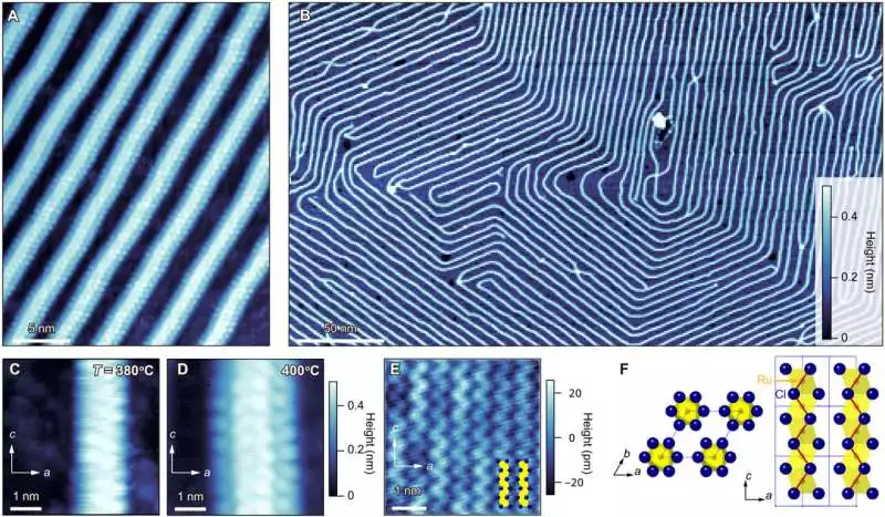
Geographical pictures of -RuCl3 nuclear-scale wires developed on exceptionally situated pyrolytic graphite (HOPG) surfaces (A) Topographic images showing the atomic structures of the four RuCl3 single-crystalline chains in the RuCl3 wires Intermittent white spots address chlorine molecules. The stated temperature is 400°C. A and B share the same color scale. (B) A topographic image of RuCl3 taken at 3 V and 20 pA on HOPG The bright lines represent four-unit cell width single-crystalline RuCl3 wires, and the dark blue areas represent a-Ru-Cl, an amorphous material made up of Ru and Cl. 400°C is the deposition temperature. (C and D) Topographic images showing the atomic structures of two and four single-crystalline RuCl3 wires, respectively. Temperatures of 380°C (C) and 400°C (D) are used for deposition. C and D share the same color scale. For (C) and (D), the images are taken at 2 V and 50 pA, respectively. E) A topographic image of a 2D monolayer of RuCl3 taken at 50 pA and 3 V, showing parallel zigzag chains of chlorine atoms. F) The -RuCl3 crystal structure as seen from the normal to the ab- (left) and ac- (right) planes The unit cell is denoted by the blue dashed lines. The monolayer crystal structure is depicted in the panel on the right. The zigzag chains of Cl atoms in E are represented by the red zigzag lines. Credit: Science Advances (2023). DOI: 10.1126/sciadv.abq5561
In this work, Asaba and colleagues used a straightforward deposition technique to create uniform, long, single-crystalline ruthenium trichloride (RuCl3) wires at the atomic scale. They produced atomically smooth junctions and nanorings, as well as a number of characteristic patterns necessary for creating quantum nanocircuits. As a Mott insulator with an energy gap created by interactions between electrons, the ruthenium trichloride material is intriguing. The team used a thin-film growth process to create and integrate the nanowire patterns, a departure from the usual strategy for atomic-scale wire patterns that encourages self-organization.
Engineering nanocircuits
During the experiments, the team used scanning tunneling microscopy to observe the result of melting ruthenium trichloride on highly oriented pyrolytic graphite surfaces using pulsed laser deposition. In order to locate a surface covered in a distinctive pattern of wires, they obtained an atomic-resolution image of a sample grown at extremely high temperatures for deposition. They observed a single crystalline structure, despite the fact that each wire had atoms that were spaced out irregularly. After extending the deposition time to grow a two-dimensional monolayer and thicker films, the materials scientists examined the material that formed the atomic-scale wires and confirmed that its composition was crystallized ruthenium trichloride.
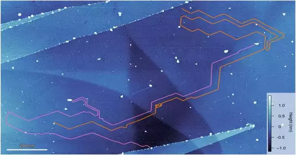
A topographic image of several micrometer-long atomic wires made of RuCl3 The orange and maroon lines are overlaid on nuclear wires of -RuCl3 with a four-unit-cell width (2.8 nm). Their lengths exceed 3 millimeters. The high groups are objects sticking to the surface, most likely during the development interaction. The geological picture was taken at 3 V and 20 D. Credit: Science is moving forward. DOI: 10.1126/sciadv.abq5561
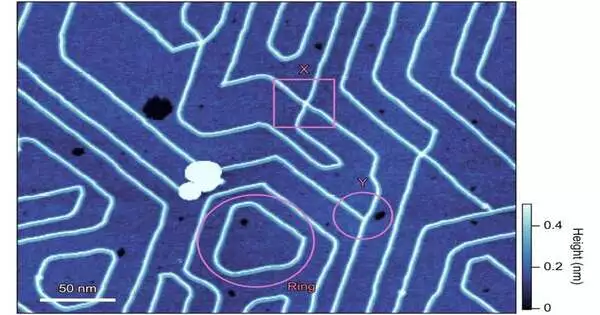
The nuclear wires kept a length surpassing 3 micrometers as a special and uncommon element. They also had two or four single-crystalline chains of ruthenium trichloride that were growing on the surfaces of pyrolytic graphite. The material’s wires started out as quadrupole chains, but as temperatures dropped, they became double chains to form atomically smooth junctions, rings without defects, and clusters in order to eventually engineer nanocircuits.
Characterizing the nanocircuits
The electronic structure of the materials was examined by measuring differential tunneling conductance, and the results were compared to those of various material forms and pyrolytic graphite surfaces. In ruthenium trichloride, they found obvious energetic gaps that pointed to electronic structures that were either semiconducting or insulating.
Through systematic band calculations of various bulk and two-chain wires, ruthenium trichloride material forms, electron correlations, and spin-orbit interactions, they discovered the source of the energy gap. In the end, the material uncovered an open energy hole at the Fermi energy across all exploratory developments utilized in the review to affirm the material as a Mott encasing.
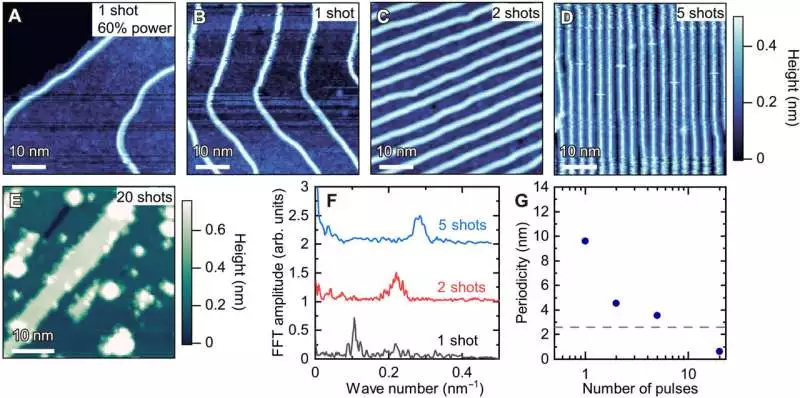
atomic-scale striped patterns of RuCl3 wires. A through D are topographic images of four-unit cell-width RuCl3 wires grown at 400°C. The wire distance can be adjusted from much longer than 10 nm (A) to shorter than 2 nm (D) by adjusting the laser’s deposition time from one shot to five shots. The force of the laser beat is additionally reduced to 60% for (A). A through D share the same color scale. E) A topographic image of a RuCl3 monolayer thin film that was grown through a further 20 shots of deposition. The regions that are green and white are, respectively, mono- and double-layer thick RuCl3. There is no 1D wire pattern visible. The setpoint conditions are 20 Dad and 3 V [(A), (B), and (E)] and 30 Dad and 3 V [(C) and (D)]. (F) Fast Fourier transform (FFT) image line profiles in the direction of the wire repetition-related peaks. The bends are upwardly moved for lucidity. (G) The periodicity, or the wave number’s opposite, is plotted in relation to the number of pulses. The four-chain wire’s width is shown by the gray dashed line. The lateral lattice constant of a monolayer of RuCl3 is represented by the data point for each of the 20 shots. Credit: Science Advances (2023). DOI: 10.1126/sciadv.abq5561.
Mechanisms of pattern formation
The team attributed the formation of the nanowire array to thin-film growth, which was distinct from any previously known process. Beside the stripe designs seen during the tests, the group examined the system’s fundamental example arrangement and the development of a few particular trademark highlights. The patterns suggested that the atomic-wire array was not driven by static interactions.
All things being equal, they attributed the component to non-harmony response dissemination processes. The team expects to take direct measurements of the dynamic process at the atomic scale in order to fully comprehend the growth mechanism because scanning tunneling microscopy is too slow to capture the dynamic processes of thin-film growth.
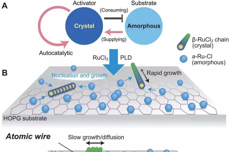
Schematic charts of the nuclear wire arrangement by the Turing instrument (A) A scheme with a substrate depleted of activators In the Turing mechanism, the conventional activator-inhibitor system, depletion of the substrate acts as an inhibitor. B and C: The process by which RuCl3 crystals form and diffuse Both sides of the 1D wires undergo the chemical reaction necessary to produce and break down RuCl3, but the side with a higher concentration of RuCl experiences the reaction more frequently. The nuclear wires proliferate toward the heading with a higher convergence of a-Ru-Cl. This interaction depicts the response dissemination at the beginning of the example arrangement. Credit: Science Advances (2023). DOI: 10.1126/sciadv.abq5561
Tomoya Asaba and colleagues hypothesized reaction-diffusion mechanisms to stimulate the origin of pattern formation in atomic wires, resulting in the manifestation of stripe patterns via Turing instability. 10.1126/sciadv.abq5561 Outlook Spatially periodic patterns spontaneously emerged as a result of the feature.
The nanowires and intersections decisively expanded the combination of electronic circuits to give an actual jungle gym to investigate the peculiarity of nuclear scale-based, non-harmony self-association appropriate for outlandish electronic states and for quantum propels.
More information: Tomoya Asaba et al, Growth of self-integrated atomic quantum wires and junctions of a Mott semiconductor, Science Advances (2023). DOI: 10.1126/sciadv.abq5561
Junhao Lin et al, Flexible metallic nanowires with self-adaptive contacts to semiconducting transition-metal dichalcogenide monolayers, Nature Nanotechnology (2014). DOI: 10.1038/nnano.2014.81


