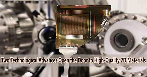
High-quality 2D materials are materials that have a thickness of only a few atomic layers, making them extremely thin and lightweight. They possess unique electronic, optical, mechanical, and thermal properties that make them attractive for a wide range of applications, including electronics, photonics, energy, and sensing.
To replace silicon in electronics with materials that offer better performance, lower power consumption, and scalability, researchers have been investigating. In order to meet this demand, a global team has created a viable method for creating high-quality 2D materials that could power future gadgets.
Sang-Hoon Bae, an assistant professor of mechanical engineering and materials science at the McKelvey School of Engineering at Washington University in St. Louis, is one of three researchers leading the multi-institutional work published Jan. 18 in Nature, together with his doctoral student Justin S. Kim and postdoctoral research associate Yuan Meng.
The work is the first to disclose that their approach of growing semiconductor materials, known as transition metal dichalcogenides (TMD), would make devices faster and use less power. It also features two technical advancements.
We believe that our confined growth technique can bring all the great findings in physics of 2D materials to the level of commercialization by allowing the construction of single domain layer-by-layer heterojunctions at the wafer-scale.
Professor Sang-Hoon Bae
The team, co-led by Jeehwan Kim, an associate professor of mechanical engineering and of materials science and engineering at the Massachusetts Institute of Technology, and Jin-Hong Park, a professor of information and communication engineering and of electronic and electrical engineering at Sungkyunkwan University, had to overcome three extremely difficult challenges to create the new materials: securing single crystallinity at wafer-scale; preventing irregular thickness during growth at wafer-scale; and vertical heterostructures at wafer-scale.
Bae said 3D materials go through a process of roughening and smoothing to become an even-surfaced material. The lack of this process in 2D materials produces an uneven surface, making it challenging to create a consistent, large-scale, high-quality 2D material.
“We designed a geometric-confined structure that facilitates kinetic control of 2D materials so that all grand challenges in high-quality 2D material growth are resolved,” Bae said. “Thanks to the facilitated kinetic control, we only needed to grow self-defined seeding for a shorter growing time.”
To produce high-quality 2D materials, there are several methods, including mechanical exfoliation, chemical vapor deposition (CVD), liquid-phase exfoliation, and molecular beam epitaxy (MBE). Each method has its own advantages and disadvantages, and the choice of method depends on the specific material and application.
By layer-by-layer growing single-domain heterojunction TMDs at a large scale, or on a wafer, the team made another technical advancement. They employed a variety of substrates made of chemical compounds to restrain the expansion of the nuclei. These substrates created a physical barrier that inhibited the development of lateral epitaxies and compelled vertical growth.
“We believe that our confined growth technique can bring all the great findings in physics of 2D materials to the level of commercialization by allowing the construction of single domain layer-by-layer heterojunctions at the wafer-scale,” Bae said.
Bae said other researchers are studying this material at very small sizes of tens to hundreds of micrometers.
“We scaled up because we can solve the issue by producing the high-quality material at large scale,” Bae said. “Our achievement will lay a strong foundation for 2D materials to fit into industrial settings.”


